August 20, 2025
As advanced electronics keep shrinking while delivering more performance, today’s advanced packaging increasingly relies on heterogeneous integration, combining multiple specialized dies into a single multi-chip module (MCM).
August 20, 2025
As advanced electronics keep shrinking while delivering more performance, today’s advanced packaging increasingly relies on heterogeneous integration, combining multiple specialized dies into a single multi-chip module (MCM).
As advanced electronics keep shrinking while delivering more performance, today’s advanced packaging increasingly relies on heterogeneous integration, combining multiple specialized dies into a single multi-chip module (MCM). From 5G transceivers to automotive radar systems, these compact, high-functionality designs are pushing the limits of wafer-level RF testing.
In this environment, fine-pitch RF calibration has become critical for keeping measurements accurate and consistent, especially at millimeter-wave frequencies above 80 GHz.
The Challenge: High Frequency Meets Fine Pitch
Modern MCMs often require electrical connections below 80 µm pitch, with operating frequencies that exceed 80 GHz. This combination makes the system far more sensitive to even small process or alignment variations, which can affect key RF parameters like return loss, insertion loss, and impedance.
When teams move to narrower pitches, a few common questions come up:
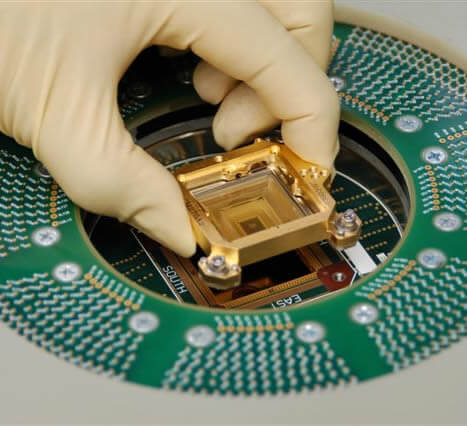
The FormFactor Approach: Precision Hardware and Controlled Experimentation
FormFactor’s Pyramid Probe delivers signal integrity up to 81 GHz, making it well-suited for fine-pitch wafer testing. To achieve accurate results, calibration is done to the probe tip using custom Impedance Standard Substrates (ISS), which match the target device geometry to minimize systematic.
At the 2025 SWTest Conference, FormFactor presented a Design of Experiments (DOE) study that evaluated how calibration responds to:
Measurements were taken with a Keysight PNA-X mmWave system up to 110 GHz, covering 864 calibration loads per ISS.
Key Findings: One Factor Stood Out
The study revealed that the pad-to-ground gap had the biggest effect on calibration repeatability and inductance stability:
This makes sense… at mmWave frequencies, even small geometry changes can have a big impact on parasitic effects.
Why It Matters for Wafer Test
For production and engineering teams, these findings point to a few practical steps:
By focusing on the variables that matter most, test teams can scale fine-pitch wafer testing for the next generation of RF devices.
Conclusion
As semiconductor devices become more complex and operate at higher frequencies, maintaining precise and repeatable wafer testing is essential. FormFactor’s work shows how better calibration design, proven probe technology, and consistent process control can deliver reliable results for today’s advanced packaging.
Download the full SWTest 2025 presentation by Daniel Bock, Ph.D. to see the detailed methodology, data, and calibration recommendations.