
March 29, 2018
Contact Intelligence enables the CM300xi to automatically adapt and adjust to provide the most accurate probe-to-pad alignment for a broad array of wafers, materials and devices.
March 29, 2018
Contact Intelligence enables the CM300xi to automatically adapt and adjust to provide the most accurate probe-to-pad alignment for a broad array of wafers, materials and devices.
The CM300xi probe station with Contact Intelligence™ technology provides research and engineering labs with an unprecedented level of automation when moving through multiple temperature points during test runs. This new technology enables probe systems to sense, learn and react to the extremely complex environments characterized by multiple temperatures and small pad layouts.
As integrated circuit products continue to move into more heat-intensive environments, such as automotive applications, it becomes increasingly critical to characterize device behavior and durability over an ever-wider range of temperatures. Previously, most chips underwent wafer-level testing at only two temperature points, typically 20˚C (room temperature) and 90˚C. Today, that range has expanded to -40˚C to 125˚C, and may involve a complete set of tests at each of four temperature steps within this range. Some cases call for even wider ranges, such as -55˚C to 200˚C, and wafer reliability testing may call for temperatures as high as 300˚C.
 This ongoing expansion in the number of required temperature steps during wafer-level testing can quickly consume a significant share of valuable lab time. The issue is compounded by the demand for increasingly large amounts of data to be extracted at each temperature step. A complete set of test cycles at all required temperature points might now take up to 72 hours, or more.
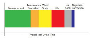
As a result, it becomes imperative to automate transitions between setpoint temperatures, automate wafer realignment at each temperature, and automate probe-to-pad realignment at each die. The figure to the right depicts the basic phases in each cycle, along with a typical apportionment of the time spent during each phase. The measurement phase includes all the time that the test probes are in contact with the wafer pads. Wafer (transition) soak refers to the interval required to reach a stable relationship between probes and wafer surface at the new temperature point. Idle time is that spent while waiting to move to the next die on the wafer, or to a new temperature set point. Die soak refers to time spent to accommodate thermal drift due to position changes. Realignment accounts for the operator input to readjust the probes after wafer soaks and die soaks.
Any approach to automating the test cycle must account for the thermal drift introduced during the wafer soak and die soak phases. Both alter the spatial relationship between the chuck, which holds the wafer, and the platen, which holds the test probes. In either case, heat-induced expansion changes their relative alignment, which in turn impacts the position of the probes on the wafer surface. During wafer soak, the chuck first reaches the required temperature, which in turn heats the platen until equilibrium is reached between the two. The time required to reach this equilibrium is called the wafer soak time.
During die soak, the heated chuck is moving between different probe locations on the wafer, which causes shifting “hot spots” on the platen. The time required to reach equilibrium with a new hot spot is termed the die soak time.
Any approach to automating and minimizing the test cycle at each temperature point must address three major issues. First, it must automate the manual realignment process required to compensate for thermal drift. Second, it should eliminate the idle time by managing the transition times and soak times with maximum efficiency by automatically realigning probes to pads after a thermal transition, or after a die step move is complete including soaking. Third, the system architecture should readily accommodate various components that minimize the impact of thermal drift at high temperatures.
We developed Contact Intelligence technology and incorporated it into the CM300xi probe system, which senses, learns and reacts to alignment issues over multiple temperatures and small pad layouts. Contact Intelligence enables the CM300xi to automatically adapt and adjust to provide the most accurate probe-to-pad alignment for a broad array of wafers, materials and devices. It applies an unprecedented level of machine intelligence to the acceleration of test cycles, while providing the highest levels of accuracy, reliability and stability in increasingly complex test environments.
For more information, visit our website, or check out the video below to see how the CM300xi probe station helps you achieve wafer-level test cycles over multiple temperatures and get results quickly.