March 16, 2018
We have a comprehensive low-frequency noise measurement solution for device modeling, characterization and reliability testing developed with our MeasureOne solution partner Keysight Technologies.
March 16, 2018
We have a comprehensive low-frequency noise measurement solution for device modeling, characterization and reliability testing developed with our MeasureOne solution partner Keysight Technologies.
As the semiconductor industry has moved to smaller devices with lower power consumption, noise plays a more significant role in overall circuit system performance. Measuring and modeling low-frequency noise becomes imperative, as this noise can impair signal processing circuitry in both signal generation and receiver circuitry. Furthermore, the industry has now adopted 1/f and random telegraph noise (RTN) metrics as leading indicators for reliability, embracing these measurements for process control in semiconductor production.
True noise immunity is essential in a measurement environment that seeks precise 1/f data from 0.03 Hz to 40 MHz. One of the biggest challenges in measuring component noise is avoiding data corruption by other noise sources in the system. Creating a noise-free measurement environment remains a costly and time-consuming pursuit for device and circuit researchers to develop on their own. Additionally, when equipment is sourced from multiple suppliers, it can be challenging to specify test system integration and performance. Measurement functionality must be validated and proven on-site before the first device can be tested, often requiring data correlation between different locations. It can take weeks, or even months to arrive at the first measurements.
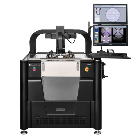
We have a comprehensive low-frequency noise measurement solution for device modeling, characterization and reliability testing developed with our MeasureOne solution partner Keysight Technologies. This solution allows us to provide semiconductor device characterization engineers a noise measurement system that integrates advanced low-frequency device noise measurement and analysis with wafer-level measurements in a single, powerful platform capable of managing full wafer-level characterization. Our Summit™ 200 mm and CM300 semi-automated 300 mm probe stations, with both probes and shielding technology, combined with Keysight’s Advanced Low Frequency Noise Analyzer and WaferPro Express software, allow a test engineer to quickly solve challenging measurement problems like device oscillation, power line noise, repeatability, and shielding from ambient radiation. This collaboration with Keysight has resulted in a fully-integrated wafer-level 1/f device characterization solution with guaranteed system configuration as well as integration, installation, training and functional on-site qualification and validation.
Our MeasureOne program offers a framework for collaboration with industry-leading partners like Keysight to offer test and measurement solutions with validated performance. Together, we can offer our customers the assurance that their complex wafer probing systems are validated and performance is optimized. Our customers benefit from faster time to first measurement and therefore faster time to market with new devices.
You can download the 1/f Device Characterization brief here or visit our website.