February 23, 2018
Silicon photonics (SiPh) is moving out of the lab and into the fab as customers demand solutions that help them accelerate their products to market and profitability.
February 23, 2018
Silicon photonics (SiPh) is moving out of the lab and into the fab as customers demand solutions that help them accelerate their products to market and profitability.
In a blog earlier this year – Two Examples of Moving Emerging Technology from the Lab to the Fab – we highlighted both high-bandwidth memory (HBM) and silicon photonics (SiPh). The first wave of the SiPh revolution stands poised to roll over data centers around the world with optical interconnects that breach the barriers set by copper wire. End user benefits might include an HD movie or 100 hours of music downloaded in a single second. Bandwidths of a terabit per second now come within practical reach.
In essence, silicon photonics merges two technologies—integrated circuits and optical communications, which have evolved along parallel but separate paths. Each offers distinct advantages. Silicon-based IC fabrication now integrates literally billions of transistors onto a single substrate. Laser-based optical communications produce very high bandwidths and low-loss signal transmission over long distances. When combined via SiPh, they offer new possibilities in transmission speed, scalability, energy efficiency and cost reduction. Over time, SiPh will scale down from data center applications to interconnects on individual chips. Eventually, hundreds of cores on a single IC could be interconnected through an on-chip optical mesh.
SiPh permits both logical and optical components to coexist on the same wafer. Optical devices such as lasers, waveguide structures, detectors, multiplexers and others could interface directly with classic logic components or can be combined as separate ICs through advanced 2.5D and 3D integration techniques. This new level of integration permits the fabrication of hybrid devices that can be mass produced and interconnected via optical fiber cabling at very low cost while yielding substantial performance gains.
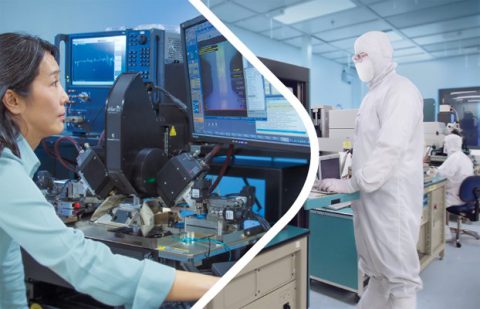
We understand the critical importance of refining and perfecting SiPh probe technology. The research at this phase of development will ultimately provide the foundation for wafer-level production test. And as SiPh technologies expand beyond the data center into a growing number of new applications, the costs associated with testing millions of devices will become a critical factor in realizing the full economic potential of SiPh.
We harness the platform’s inherent capabilities and extend them through a new software package, SiPh-Tools, to provide a system-level solution for SiPh wafer test. SiPh-Tools interfaces with third-party probe control software to accurately place optical fibers with sub-micron level precision. On the instrumentation side, we facilitate the interaction with Keysight’s Photonics Applications Suite, which controls the actual measurement functions, such as laser beam generation and optical power detection, along with standard electrical measurements.
This type of multi-partner effort is already producing a deep knowledge base, the kind that will move silicon photonics out of the lab and into the fab as customers demand solutions that help them accelerate their products to market and profitability.
For more information, download the technical brief Moving Silicon Photonics Out of the Lab and Into the Fab.