Adoption of advanced packaging is accelerating as the benefit of the classic Moore’s Law transistor shrink diminishes on a monolithic die. Advanced packages enable the heterogenous integrations of multiple different die through high-density interconnects, for improved device performance and smaller footprint. Advanced packaging architectures like Intel’s Embedded Multi-Die Interconnect Bridge, TSMC’s Integrated Fan-Out, and High Bandwidth Memory (HBM) have taken up the slack from Moore’s Law in order to meet the demands for greater connectivity, computing power, speed, and cost-effectiveness of megatrends in transportation, 5G, IoT, artificial intelligence, and high-performance computing. Advanced packages have enabled the industry to develop new flip-chip processes, 2.5D interposer and TSV technology, and most recently, 2D and 3D fan-out processes with high densities of connections in the smallest of spaces.
Fan-out Wafer Level Packaging (FOWLP) is one of the fastest growing advanced packaging segments today. According to Yole Research, FOWLP is expected to grow to $2.5B by 2022, up from $320 million in 2016. In FOWLP, individual chips are assembled into an artificial wafer made of low-cost polymer materials with additional space for connections. An RDL redirects the connections on the chip to the edge areas. The advantages of FOWLP include improved performance per watt and a wider range of different designs due to thinner packages, but the manufacturing of these new devices present new measurement challenges, including the ability to measure deep etch trenches.
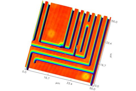
The established devices of the MicroProf® series in combination with the white light interferometers WLI PL and WLI FL, offer optical and non-contact innovative solutions in the field of advanced packaging for production, research and development where other processes reach their limits. For example, plasma diced etch trenches have depths of 50 to 200 µm, which are far beyond the reach of AFM or profilometer tips. Many optical methods such as confocal microscopy are also not suitable for this measurement due to their aperture, as no light from the bottom of the trenches can get back into the sensor due to the shadowing of the side walls. In addition, the etching process leads to a roughening of the surface in the etching trenches and thus to high differences in the reflectivity between the substrate surface and the bottom of the trenches, which can lead to problems during measurement.
Thanks to its parallel illumination, the WLI PL is excellently suited for the measurement of plasma diced etch trenches with a high aspect ratio, since a large proportion of the light reaches the bottom of the etching structure and the depth can thus be measured. Depending on the surface texture, structures with minimum widths from 2 to 3 µm and aspect ratios of up to 50:1 (depth to width) can be measured. The use of a special measuring mode enables the measurement in two measuring steps. The substrate surface and the bottom of the structures are measured in such a way that an optimal adaptation of the measuring parameters to the different surface conditions is achieved.
Another problem for measurement technology is often the small lateral dimension of the structures, since the optical resolution of the methods is usually not high enough. Trenches, for example, can have trench widths of less than 1 µm. The WLI FL uses a special algorithm to determine the depth of etching structures down to 0.7 µm in width. In this case, the aspect ratio can be up to 3:1. This allows access to dimensions that have not been reached before. This method makes it possible to measure all currently used variants of TSVs, including vias with diameters of less than one micrometer that are no longer optically detectable.