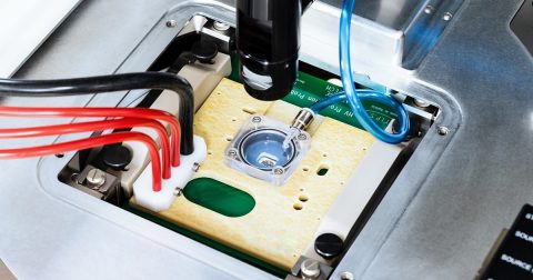
High-voltage/high-current semiconductor development is ramping up, thanks in part to electric vehicles and other applications gaining momentum. Wafer tests of these power semiconductors is fraught with challenges; the result of test currents exceeding 500 Amps and voltages up to 10 Kilovolts.
There’s a megatrend taking place in power electronics. While the total power market is experiencing CAGR growth of +4.3%, the EV/HEV power market is experiencing CAGR of +21% (Yole Development). The broad use of power semiconductors has created a pressing need to characterize power devices quickly and efficiently. The challenges with of measurements on-wafer instead of in-package creates major challenges in collecting accurate data:
- Probe and system anti-arcing at high voltage
- Low resistance probe and wafer contacts for high-current
- Special handling for thinned wafers
- Quick and easy setup of complex high-power test configurations
- Operator and device safety
Be sure to watch the on-demand webinar from Eric Wilcox and Rainer Gaggl as they showcase the TESLA power device characterization system and T.I.P.S. high-voltage “LuPo” probe cards. TESLA probe systems are optimized for the complex challenges of on-wafer high-voltage and high-current measurements. TIPS “LuPo” probe cares complement TESLA probe systems with capabilities for arc-free high-voltage probing. Together they overcome the challenges above resulting in highly accurate data when probing high-voltage/high-current devices.
You can watch the on-demand webinar here.