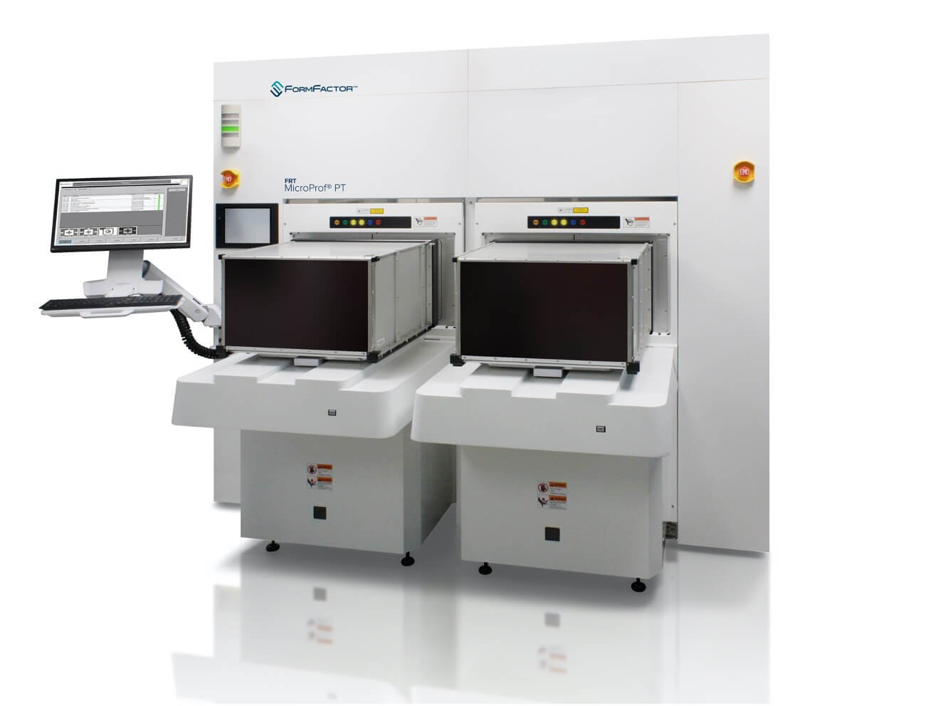
FormFactor is pleased to introduce the FRT MicroProf PT, a new semiconductor metrology and inspection tool for rectangular panels up to 600mm containing 4-5X more dies compared to a 300mm wafer. With full automation and hybrid metrology capabilities, a single automated system can perform multiple types of 3D measurements and defect detection on the high-capacity panels to efficiently accelerate the processing of important new advanced package technologies such as fan-out panel-level packaging (FoPLP).
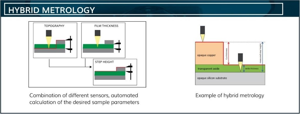
FoPLP and other advanced package techniques stack several semiconductor dies into a single heterogeneous package using connection elements such as microbumps, TSVs (through-silicon vias), and interposers. In device development, the new FRT MicroProf® PT with SurfaceSense™ technology incorporates a variety of high-precision sensor options to measure the filigree shape and critical dimensions of these inter-die connections, as well as thickness, roughness and other characteristics of the film and metal layers that make up each device. Fully integrating into factory floor automation, the tool can also deliver essential defect inspection data for process control and yield improvement. Equipped with our SurfaceSense™ technology, the FRT MicroProf® PT supports the development of these new packaging processes on panel level. This gives our customers the flexibility to use the tool both in development and production. The novel panel technology means a significant increase in the surface area that can be processed into chips in a single pass. It also allows the processing of much thinner chiplets and simplifies packaging.
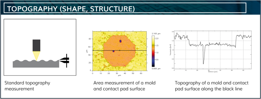
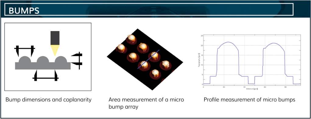
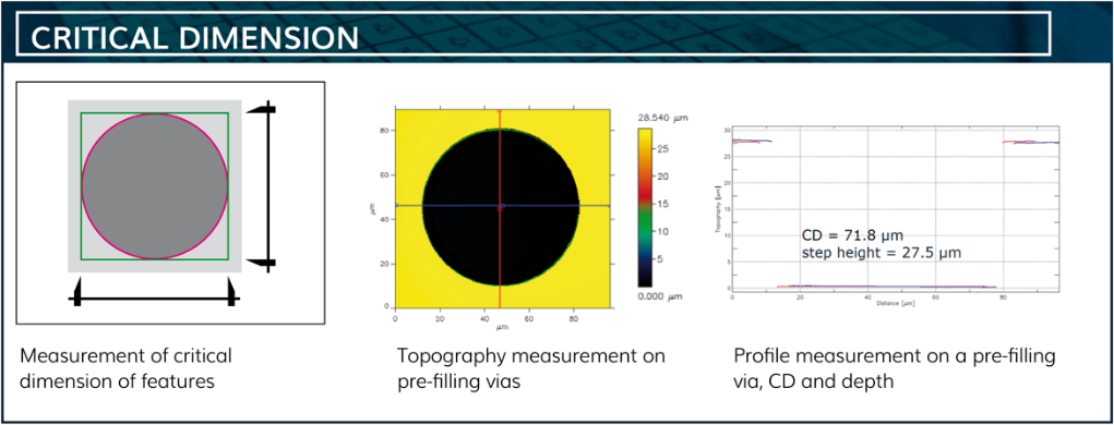
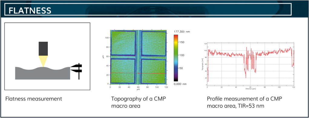
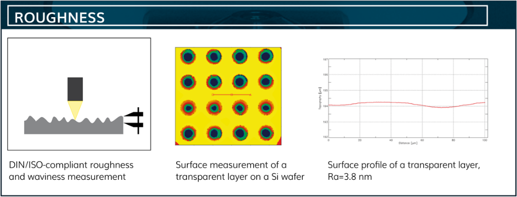
Some application samples:
For a measurement, the samples must be moved under clean room conditions (absolutely dust-free), very quickly and very precisely. Due to their formfactor, this requires more effort with the comparatively bulky panels than with wafers. Our EFEM tool for panels is designed for panel dimensions up to 600 x 600 mm and thicknesses between 200 μm and several millimeters.
The MicroProf PT is the latest addition to our Advanced Packaging metrology product family, and compliments the MicroProf AP, a now-established wafer-level packaging solution. Key features include:
- Metrology and defect inspection applications in one tool
- Full automation with two loaders for panel FOUPs
- Ability to handle any size panel up to 600mm x 600mm
- Multi-sensor setup including topography point sensors, field-of-view and film thickness sensors and hybrid software evaluation to evaluate highly complex structures
- Film thickness measurements from micron-range down to tens of nanometers
- Wide range of handling capability – from substrates a few millimeters thick to 200µm
- Support for various substrate materials, including organic and glass
- Complete production floor integration with SECS/GEM protocols
Thomas Fries, Vice President and General Manager of FormFactor’s Emerging Growth Business Unit states:
Since process and system development for panel technologies is ramping up, direct adoption of wafer-level materials, technologies and standards is not possible in most cases. Equipped with our SurfaceSens technology, the MicroProf PT supports the development of these new packaging processes on panel level. This gives our customers the flexibility to use the tool both in development and production.
To learn more about MicroProf PT, be sure to visit our website.