October 24, 2025
Based on FormFactor’s IEEE-published research, this optical system maintains alignment accuracy over long test cycles and varying environmental conditions, ideal for production environments.
October 24, 2025
Based on FormFactor’s IEEE-published research, this optical system maintains alignment accuracy over long test cycles and varying environmental conditions, ideal for production environments.
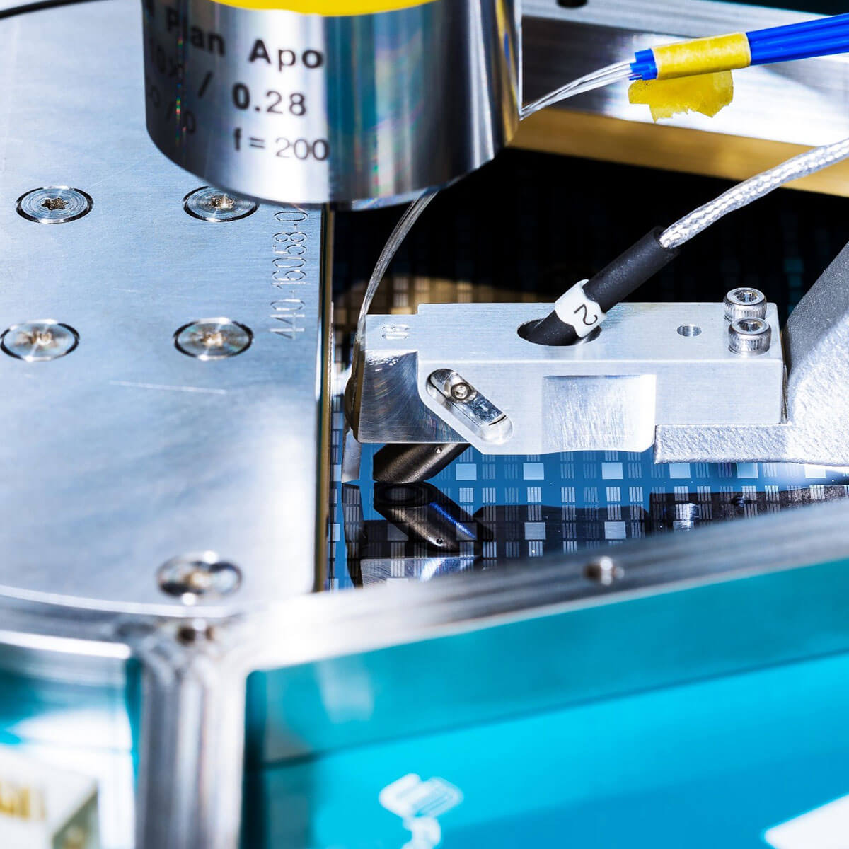
In the fast-moving world of silicon photonics, wafer-level testing has become essential. As photonic integrated circuits (PICs) power everything from data communications to AI acceleration, the industry faces a persistent challenge: achieving accurate, repeatable optical measurements directly at the wafer level.
Manual alignment during SiPh probing often leads to inconsistent results. Traditional approaches like tapered lensed fibers are prone to misalignment, high insertion loss, and even physical damage to chip facets. These limitations make it hard to scale optical testing from the lab to high-volume manufacturing.
That’s where the Pharos Probe Series comes in. Designed by FormFactor, Pharos delivers automated wafer-level edge coupling with per-facet losses of less than 1.5 dB. By combining precision optics, stable mechanical design, and automated alignment, Pharos eliminates one of the biggest bottlenecks in silicon photonics testing.
Pharos brings together automation, repeatability, and high optical performance to transform wafer-level photonics testing. When paired with the CM300xi-SiPh Probe Station, engineers can perform fully automated optical and electrical measurements across entire wafers, saving time and improving consistency.
With Pharos, you get:
By automating fiber alignment and calibration, engineers can now take thousands of measurements per wafer with minimal manual intervention. What used to take hours can now be done in a fraction of the time, with repeatable, reliable results every step of the way.
No two photonic devices are exactly alike, and test setups shouldn’t be either. The Pharos probe is built for flexibility, supporting both edge-coupling and vertical-coupling configurations. It’s compatible with a range of fiber types, pitch sizes, and channel counts.
This flexibility allows engineers to customize their setup to match any device, from single-channel R&D prototypes to high-volume wafers with dozens of optical ports. Whether you’re developing next-generation optical interconnects or validating new SiPh architectures, Pharos provides a scalable, adaptable solution that grows with your testing needs.
Advanced Optics and Robust Engineering
The innovation behind Pharos comes from its precision lens system and rugged mechanical architecture, which together deliver ultra-low-loss coupling without sacrificing alignment speed or reliability. Based on FormFactor’s IEEE-published research, this optical system maintains alignment accuracy over long test cycles and varying environmental conditions, ideal for production environments.
Each element of the Pharos system, from the optical ferrule to the mechanical interface, is engineered for:
This attention to detail results in a robust, stable system that supports high throughput and uptime across demanding test programs.
As data centers and high-performance computing systems move toward co-packaged optics, the need for scalable optical wafer test solutions has never been greater. Photonic and electronic components are increasingly integrated on the same substrate, demanding precise alignment between optical and electrical domains.
The Pharos probe helps bridge that gap. It enables repeatable, wafer-level optical testing that supports the development of co-packaged optics, heterogeneous integration, and 3D photonic-electronic architectures. For device makers, that means faster development, higher yields, and lower costs, all while maintaining the performance required for the next generation of bandwidth-intensive applications.
Integration with the FormFactor Ecosystem
Pharos is part of FormFactor’s complete silicon photonics testing ecosystem, which includes:
Together, these solutions create a fully integrated environment for photonic wafer testing, from early R&D to high-volume production, ensuring consistency and confidence at every step.