As the demand for high-speed data processing and low-latency communication continues to grow, silicon photonics (SiPh) has emerged as a foundational technology in applications ranging from 5G and data centers to quantum computing and LiDAR. However, a persistent bottleneck in silicon photonic device manufacturing has been the lack of a scalable, repeatable wafer-level edge coupling solution… until now.
At FormFactor, our engineers have collaborated with IHP Microelectronics to develop the industry’s first fully automated wafer-level edge coupling measurement system designed specifically for silicon photonic integrated circuits (PICs). This breakthrough raises the bar for wafer testing, delivering faster automation, better coupling efficiency, and measurement consistency.
Why Edge Coupling Matters in Wafer Testing
Traditionally, grating couplers have been used for wafer-level optical testing. While simple, they suffer from bandwidth limitations and polarization dependence, limiting their utility in advanced applications. In contrast, edge coupling offers broad bandwidth, low loss, and minimal polarization issues, making it ideal for high-performance photonic devices. Yet, wafer-level edge coupling has long been constrained by mechanical challenges, alignment difficulties, and probe fragility.
This is where FormFactor’s innovation stands apart.
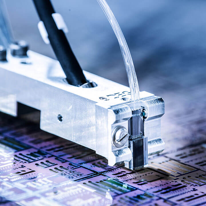
At the heart of our system is the Pharos lens, a micro-fabricated optical probe built using two-photon lithography to achieve nanometer-scale resolution. Its periscope structure converts vertical light into a horizontal beam path, enabling efficient in-plane coupling with silicon waveguides. Testing on 200 mm wafers demonstrated coupling losses as low as 1.51 dB/facet, outperforming cleaved fiber arrays and maintaining high efficiency across a range of working distances.
Key features of the Pharos lens include:
- Customizable Mode Field Diameter (MFD) for better waveguide matching
- Compatibility with both trench and V-groove wafer structures
- A non-background-impact fiducial for precise machine-vision alignment
This advanced measurement solution is built around the FormFactor CM300xi probe station, integrating:
- eVue Microscope System for sub-micron resolution imaging
- Vuetrack Control Algorithm for error compensation and drift correction
- Adaptive Optics and Gradient Search Algorithms to optimize alignment and reduce test time to under 5 seconds per die
The result? Repeatable measurements with less than 0.2 dB variation and stability that stay within 0.01 dB, even during extended test sessions.
Edge vs. Grating, Comparative Test Results
Extensive wafer-level testing was conducted on photodiode structures fabricated using IHP’s 0.25 µm photonic BiCMOS process. Comparison between edge and grating coupling showed nearly identical photodiode responsivity:
- Edge coupling, 0.75 A/W
- Grating coupling, 0.79 A/W
These results show that automated edge coupling performs just as well, if not better, than vertical methods, with the added benefit of being ready for real-world packaging.
This system is a game changer for testing the kinds of devices driving the future, like 5G transceivers, quantum photonics, AI accelerators, and LiDAR for autonomous vehicles.
By enabling high-throughput, production-grade testing of edge-coupled devices, it accelerates time-to-yield and reduces test costs across the photonics manufacturing lifecycle.
Learn More
Explore how FormFactor is shaping the future of wafer-level test:
For more technical insights, you can also read the full IEEE article here, IEEE Transactions on Semiconductor Manufacturing, May 2025