March 9, 2026
For years, wafer test was treated as a line item to minimize. That thinking breaks down when die sizes grow, AI accelerators get more complex, and scrap costs skyrocket. One bad die that escapes into a package can have a huge impact.
March 9, 2026
For years, wafer test was treated as a line item to minimize. That thinking breaks down when die sizes grow, AI accelerators get more complex, and scrap costs skyrocket. One bad die that escapes into a package can have a huge impact.
When people talk about AI hardware, the conversation usually jumps straight to GPUs, HBM stacks, and cutting-edge fabs. In a recent Advantest Talks Semi episode, host Keith Schaub and FormFactor Chief Commercial Officer Aasutosh Dave stepped back and focused on something much closer to the wafer: the probe card and the role of wafer test in getting known good die into the supply chain.
If you work in yield engineering, test, or high-volume manufacturing, their discussion makes one thing very clear: wafer test has moved from “necessary expense” to “strategic enabler” in the AI era.
A career that spans the entire semiconductor flow
Aasutosh brings an unusually broad view to the conversation. He started in India as an R&D lithography process engineer, owning critical process layers at AMD. From there he moved into computational lithography and DFM/OPC at Mentor Graphics, then into metrology and inspection leadership at ASML.
That path, from front-end process to design enablement to defect inspection, eventually led him to FormFactor and back-end test and measurement. It’s why he doesn’t see front end and back end as separate camps at all. In his view, everyone is serving the same ecosystem, and the back end is receiving increased attention as its complexity and importance grow.
Wafer test is no longer a commodity
For years, wafer test was treated as a line item to minimize. That thinking breaks down when die sizes grow, AI accelerators get more complex, and scrap costs skyrocket. One bad die that escapes into a package can have a huge impact.
In the podcast, Aasutosh calls out three big shifts:
Instead of being the bottleneck at the end of the line, wafer test is increasingly part of the design conversation from the start.
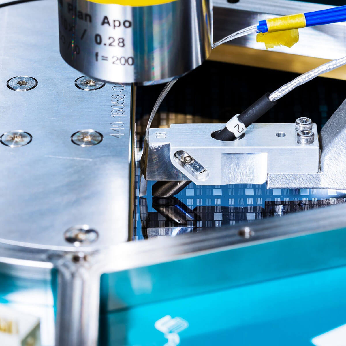
What today’s probe cards are really doing
One of the most eye-opening parts of the discussion is just how extreme modern probe requirements have become.
On the memory side, especially for HBM, FormFactor’s SmartMatrix 3D MEMS solutions are designed to handle:
It’s not unusual to be talking about a hundred thousand pins or more, often across multiple dies, with customers pushing hard for one-touchdown solutions.
For logic SoCs, the picture is different but just as demanding. You’re typically probing one die at a time, but still with tens of thousands of pins and aggressive multi-site strategies, 4x, 10x, 16x sites, to bring down cost of test.
Then there are RF, automotive, and mobile devices, which bring their own constraints. Here, FormFactor uses flexible-substrate Pyramid probes and a mix of 2D, 3D, and flex architectures optimized for RF performance, reliability, and signal integrity.
The common thread: there is no one-size-fits-all probe. Each application class needs its own architecture and trade-offs.
From lab to fab: silicon photonics and co-packaged optics
The conversation then shifts to silicon photonics and co-packaged optics. As Keith points out, data centers are full of copper and power-hungry links. Moving to optical I/O isn’t a nice future idea anymore, it’s quickly becoming a requirement.
Aasutosh describes how this is changing test:
This is where the “lab-to-fab” concept shows up in a concrete way. Capabilities proven in R&D tools, like precise optical alignment and advanced thermal management, are making their way into production probe cards so they can scale with AI and hyperscale computing demands.
Uptime, service, and the real KPIs in production
Anyone who has run a high-volume test floor knows that technology specs are only half the story. Uptime, service, and logistics matter just as much.
Aasutosh explains that when a probe card fails, wafers simply stop moving. That’s direct cost and lost production opportunity. To stay ahead of that, FormFactor puts a lot of emphasis on:
To support these expectations, FormFactor has built out service centers in key regions, recently doubled capacity in Taiwan, and added a new factory in Farmer’s Branch, Texas, with large cleanroom capacity to help reduce lead times and support future growth.
For operations and test managers, the message is simple: advanced probe technology only helps if it’s available, stable, and supported where you run.
“Pin Count Prophecies”: future ideas vs real roadmaps
Keith also shares a fun segment where he asks ChatGPT to predict future probe innovations, then checks them with Aasutosh. The ideas range from “interesting” to “definitely sci-fi”:
The point isn’t to predict specific products, but to highlight that real innovation in probe technology has to respect materials, manufacturing, and economics, not just imagination.
What this means for your test and product roadmap
If you’re planning next-generation AI accelerators, HBM stacks, or advanced packages, the takeaways from this conversation are clear:
If this discussion sparks ideas about your own wafer test challenges, FormFactor can help you explore probe solutions that match your roadmap for AI, memory, RF, and silicon photonics.