As AI workloads, high-performance computing (HPC), and hyperscale data centers continue to push the limits of bandwidth and energy efficiency, silicon photonics has become a critical enabling technology. But as devices transition from research to production, the demands on wafer test methodologies grow just as quickly.
Test approaches designed for R&D don’t always hold up in high-volume manufacturing, where throughput, repeatability, and automation become critical. TRITON™ changes that equation.
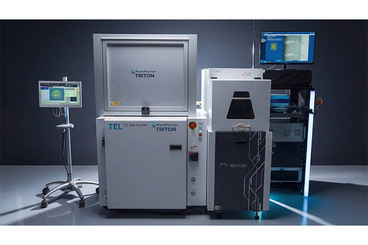
Purpose-built for production, TRITON is the industry’s first fully integrated silicon photonics test cell, delivering the precision engineers expect in the lab with the scalability required on the fab floor.
Bridging the Gap Between R&D and Production Wafer Test
For more than a decade, FormFactor has supported silicon photonics innovation with platforms like the SUMMIT200-SiPh and CM300xi-SiPh. These systems helped define how engineers perform high-precision wafer-level testing in R&D environments.
But moving into production introduces a different set of challenges:
- Maintaining measurement accuracy at scale
- Reducing setup and calibration time
- Ensuring repeatability across thousands of wafers
- Integrating into automated fab environments
TRITON is built to solve these challenges, making it easier to move from development into high-volume wafer testing without reworking your entire test approach. It gives teams a consistent path from early device validation to full-scale manufacturing.
A Production-Ready Silicon Photonics Test Cell
TRITON goes beyond a traditional probe station; it’s a fully integrated wafer test solution built for real manufacturing environments.
Developed in collaboration with Advantest and Tokyo Electron (TEL), TRITON brings optical probing, electrical testing, automated wafer handling, and factory automation together into a single, synchronized platform.
By bringing everything into one system, TRITON removes the complexity of fragmented test setups. Instead of stitching together multiple tools and workflows, engineers can rely on a unified platform that improves throughput while maintaining consistency from wafer to wafer.
Automated Photonic Alignment with Nano-Precision
One of the biggest challenges in silicon photonics wafer testing is getting optical alignment right. Even small inconsistencies can impact measurement accuracy and yield.
TRITON addresses this with nine-axis nano-precision alignment, enabling:
- Highly accurate fiber-to-device positioning
- Consistent alignment across wafers and production runs
- Reduced operator intervention
With coupled-power repeatability within 0.3 dB, engineers can trust the stability and reliability of their measurements.
This level of precision comes from advanced vibration isolation, robust mechanical stability, and automated alignment routines. The result is a system that delivers lab-grade accuracy, even at production scale.
Flexible Optical Coupling in a Single Platform
Silicon photonics device architectures continue to evolve, and test strategies need to evolve with them.
TRITON supports both edge and surface coupling within the same system, allowing engineers to work with grating-coupled, trench-based, and edge-coupled devices without switching setups. Integrated with FormFactor’s Pharos™ optical probe, the platform enables ultra-low-loss edge coupling directly at the wafer level.
By combining these capabilities into a single test cell, TRITON removes the need for multiple setups, simplifying workflows and cutting down test time as device designs change.
Fully Automated Optical and Electrical Co-Measurement
Modern silicon photonics devices require tightly synchronized optical and electrical testing. TRITON integrates directly with Advantest’s V93000 (93k) platform to enable fully automated co-measurements within a single test flow.
With everything tightly integrated, engineers can run complex test sequences with minimal manual work. Calibration, optical scanning, and measurement can all be executed within a single automated flow, improving repeatability across wafers and test cycles.
This level of automation not only increases throughput but also helps eliminate variability introduced by manual processes.
High-Density Wafer Testing for Production Efficiency
As silicon photonics moves into high-volume production, test efficiency becomes a major factor in overall manufacturing cost and yield.
TRITON supports high-density configurations, including:
- MF80 and MF130 probe cards
- Optical fiber array units (FAUs)
- Parallel device testing across the wafer
High-density wafer probing is key to scaling silicon photonics manufacturing, especially for applications like AI interconnects and co-packaged optics where performance and volume both matter.
Built for Factory Automation
TRITON is designed to fit seamlessly into modern semiconductor fabs and OSAT environments.
It supports overhead transport systems (OHT), integrates with SECS/GEM factory automation standards, and enables automated binning and data tracking. These capabilities allow TRITON to operate as part of a fully automated production line, delivering consistent, repeatable wafer testing at scale.
Rather than adapting a lab tool for production, TRITON is engineered from the ground up to meet the realities of manufacturing.
Software That Simplifies Complex Workflows
Behind TRITON’s performance is a powerful set of software tools designed specifically for production environments.
- SiPh Tools manages wafer-level optical workflows, calibration routines, and high-density test execution
- TritonConnect simplifies operator interaction with automated alignment, micro-positioning, and system control
Together, these tools help shorten test time while still delivering the precision required for next-generation silicon photonics devices.
Enabling the Next Wave of AI and Data Center Innovation
Silicon photonics is at the heart of some of the most demanding applications in the semiconductor industry today.
- AI and machine learning infrastructure
- Co-packaged optics (CPO)
- High-speed data center interconnects
- High-performance computing (HPC)
These applications require wafer test solutions that can deliver both precision and scale. TRITON is designed to meet these demands by combining nano-precision alignment, low-loss optical probing, synchronized co-measurement, and full factory automation.
Why TRITON Matters for Wafer Test Innovation
Wafer testing plays a critical role in improving yield, reducing defects, and ensuring device reliability across semiconductor manufacturing .
TRITON advances wafer test by:
- Unifying optical and electrical testing in one platform
- Reducing variability through automation
- Increasing throughput without sacrificing accuracy
- Enabling scalable, production-ready workflows
For engineers and manufacturers, that translates into faster time-to-market, better yield, and more confidence in device performance.
Production-Ready Silicon Photonics Testing—Engineered to Scale
TRITON marks a major shift in how silicon photonics devices are tested at the wafer level.
By bridging the gap between R&D and high-volume manufacturing, it gives teams a scalable, automated, and consistent approach to wafer testing, without compromising precision.
In an industry where performance, reliability, and speed are everything, TRITON provides the foundation for next-generation silicon photonics manufacturing.