Terahertz (THz) technologies are often bulky and expensive systems used only for radio astronomy and lab applications. Today, however, the technical progress achieved in recent years makes it possible for THz technologies to be commercialized in markets for inspection, control and monitoring, non-destructive testing (NDT), and for industrial monitoring of processes such as pharmaceutical quality control (QC). In addition, because of their ability to penetrate through barrier materials such as clothes and packaging, non-contact and non-ionizing testing can also be performed. THz technologies are also expected to open new applications, especially in biomedical, homeland security and telecommunications, which will become the drivers of THz market growth in five to ten years.
While significant progress has been made in THz (300-3000 GHz) circuit fabrication, with more power available at higher frequencies, the measurement infrastructure for characterizing such components remains largely undeveloped. The challenges range from the technical; integration, high transmission line losses and machining tolerances to the administrative, with no broadly accepted standards.
Continued growth in THz applications requires the availability of quality test and measurement equipment. Typically, individual devices must be diced and mounted to a fixture for measurement. Robust and calibrated on-wafer measurements of planar millimeter and sub-millimeter wave devices would significantly reduce the effort required to characterize a wafer of devices while increasing the accuracy of the measurement by eliminating errors and effects associated with fixtures.
To configure a system to meet these challenges you must specify and source instrumentation, wafer probe stations, probes, standards and calibrations software from multiple suppliers and then integrate and prove these onsite before your first device can be tested. It can take weeks, or even months, before you can execute your first measurements with any confidence that there is data correlation and measurement accuracy with day to day repeatability.
For engineering lab and production customers who need quick access to the best products to meet their test and measurement requirements, we’ve created our MeasureOne™ solutions program. MeasureOne is a unique commitment between us and our best-of-breed partners to streamline their processes and realize efficient, “true to measurement” solutions. MeasureOne solutions will be validated to ensure all components of the solution will work together with seamless integration. In many cases, performance will be qualified with extensive testing and characterization, and the solution will be verified after installation.
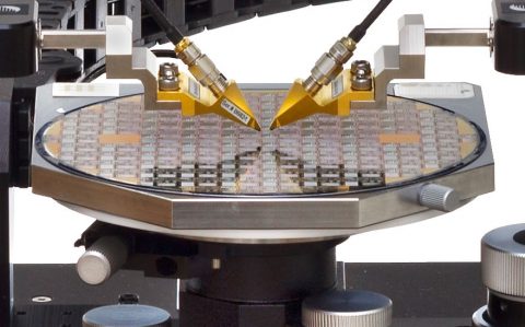
Under the MeasureOne program, our collaboration with DMPI allows us to provide millimeter and sub-millimeter wavelength on-wafer ground-signal-ground probes and associated components for electrical measurement of devices and materials with frequencies from 140 GHz to 1.1 THz. The probes offer low insertion loss, as well as excellent probe tip and sample visibility. For THz measurements at the probe tip, the importance of probe placement onto the calibration standards is critical. In order to make accurate and repeatable measurements above 500 GHz, probe placement errors need to be less than 1 μm, and this is challenging to achieve with a manual probe station and positioners. Our Summit™ and CM300™ semi-automated probe stations can be configured with programmable positioners to allow rapid and repeatable sub-micron positioning accuracy to ensure the highest precision at the probe tip during an automatic Multi Line TRL calibration. The THz probe products will be validated on our EPS150mmW manual probe station, as well as the Summit200, and the CM300 on-wafer probe systems.
For more information on MeasureOne solutions, check out our website.