We’ve previously blogged a about the numerous benefits of our Contact Intelligence™ technology: Transforming 300 mm Probing with Contact Intelligence Technology
CM300xi Wafer Probe Station with Contact Intelligence Aids High-Volume Engineering
Recently, we announced that we have extended our Contact Intelligence technology to handle Autonomous RF, Autonomous DC, and Autonomous Silicon Photonics (SiPh). With Contact Intelligence we provide Autonomous Measurement Assistants, which will enable faster time to data.
- Autonomous RF: New high frequency IC’s, such as 5G (with multiple high frequency bands from sub-6 to more than 70 GHz) and automotive communication devices, need the highest quality process design kits (PDK’s) to ensure working devices at first iteration. Traditional systems and methods require engineers to invest significant time for recalibration when the system invariably drifts, or to reposition probes with intentional changes in test temperatures. At higher frequencies, calibrations and measurements are more sensitive to probe placement errors and there is more calibration drift, so recalibration is required more often. Over time and temperature, Contact Intelligence automatically makes these adjustments with no operator intervention, resulting in more devices tested in less time, for more accurate PDK’s and faster time to market.
- Autonomous DC: In DC applications, Contact Intelligence automatically senses preset temperatures, and responds by waiting the correct amount of time until the system is stabilized. This allows lengthy test routines to be conducted over multiple temperatures without an operator present. Contact Intelligence also provides dynamic probe-to-pad alignment, even on pads as small as 25 µm, employing a combination of smart software, probe tip recognition algorithms and advanced programmable positioners.
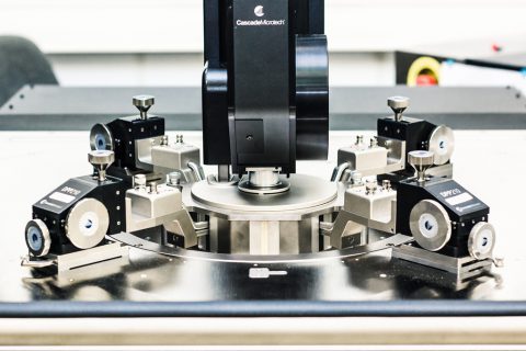
- Autonomous SiPh: Our integrated SiPh solution allows sub-micron manipulation of optical fibers positioned above the wafer, automatically optimizing fiber coupling position. Contact Intelligence uses machine vision technology to automate Theta X, Y and Z axis calibrations and alignments enabling measurements out of the box, reducing what used to take days or weeks to a matter of minutes. When combined with autonomous DC and RF, measurement options expand from Optical-Optical to include Photo-Diodes, Optical Modulators and more.
Trends in the semiconductor industry continue to point to the shrinking of feature size, scribe lines and smaller pad sizes as our daily devices get smaller and more complex. In device characterization and high-volume engineering applications there is an increasing need to reduce operator intervention by automating thermal transitions and probe-to-pad realignment, enabling “unattended” test over multiple temperatures. The twin challenges brought on by expanding temperature ranges and shrinking feature sizes can significantly prolong the time required for accurate probe placement during many types of wafer-level testing.
With Contact Intelligence, our advanced probe systems now automatically and autonomously adapt in real time to changes in the testing environment, enabling customers to collect large amounts of RF data faster. As the race to bring 5G devices to market heats up, this addresses the need for higher productivity, to reduce time to market.
You can explore Contact Intelligence on our website or download the solution briefs below: