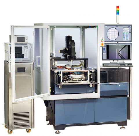
We’re excited to showcase our new TESLA200 high-power semiconductor probing system. This system is designed specifically for IGBT and power MOSFET device measurements. The demand for high-power devices (built on Si, GaN and SiC substrates) has been primarily driven by automotive and industrial segments such as hybrid and electric vehicles, solar, transportation, data center power supplies, and other industrial segments. Combining next-generation test capabilities, with anti-arcing solutions and wafer automation, the TESLA200 enables wide thermal range and fully automatic thin and warped wafer loading and can provide accurate data at up to 10,000 V and up to 600 A current.
The TESLA200 allows engineers to collect data on individual or volume wafers, providing faster characterization and shorter time to market. Some of the key features of this new high-power probe system include:
- Flexible, thin wafer handling:
- Full-auto wafer handling – Cassette and manual loading, safe robot handling for thin or warped wafers, and you’ll save time with parallel ID reading and pipelining.
- Time saving test “recipes” – Fast loading and unloading of the wafer to a hot or cold chuck, easy operation with new software, and stored information for wafer and end effector types.
- Thin and standard wafers – MicroVac technology for the best thermal and electric accuracy with standard, thinned, or TAIKO wafers (down to 50um).
- Accurate data measurements:
- New MicroChamber™ – This contributes to more to more accurate measurements and easier operation. For example, it provides new top hats to open the space for easier probe setups and smoother integration of instruments. There is also a new safety door lock which prevents the user form accidentally icing the wafer at cold temperatures.
- Integrated HTS (High Thermal Stability) – HTS is now integrated into every prober configuration with a thermal system. This reduces soak time and provides repeatable probe contact and is a part of the Contact Intelligence™ technology for small pad probing.
- High accuracy IV and CV measurements – Leading measurement technologies like PureLine or AttoGuard enable higher signal to noise ratios, lowest error measurements and reduced settling time for faster accurate measurements.
- Supports high volume engineering and niche production requirements:
- Solutions for every high-power application – Supports 3kV, 10kV, 200A, and 600A.
- Faster time to first data – Our SIGMA kits contain all the necessary application layer accessories to integrate an instrument or application with our probe system and help you achieve maximum measurement performance right away.
- Modular system design:
- TESLA200 is based on a newly developed modular core system – There are 3 base model default configurations and 2 automation levels. Starting from these 6 base configurations you can de-select, replace or add modules. This helps to tailor the system to the customer needs.
- Saves money – The modularity enables you to even generate “low budget” configurations with much less features then the base model.
- Faster customization – The modularity also helps to speed up the customization process and reduces service efforts due to the standardizing of interfaces.
- Superior scalability:
- Field upgradable – Due to the standardizing of interfaces between the various modules, it is now possible to scale the system easily. If you are changing over time, many modules can be later upgraded in the field.
- Test accuracy upgrades – Test accuracy features like the MicroChamber, ThermalSystems, AttoGuard/Pureline technology or autonomous RF probing.
In addition to these improved features and benefits, the TESLA200 is been designed for improved quality as well as performance. This has been achieved by continuous product improvements efforts, ISO9001 certified processes and stronger manufacturing processes.
For details on the new TESLA200 high power probe system, check out our website or download the data sheet (PDF).