The EPS150RF and EPS200RF probe systems are application-focused packages that offer complete solution for best-in-class RF measurement results. Based on leading technology in RF probing and probe system design, and over 30 years of experience and application expertise, these solutions are the key to achieving accurate measurement results in the shortest time—with maximum confidence.
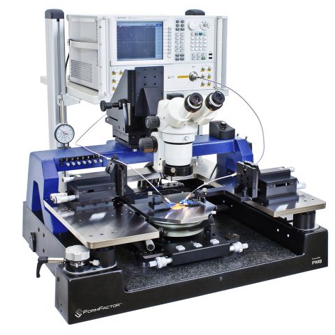
The EPS150RF package is based on MPS150 150 mm probe station platform and the EPS200RF package is based on the PM8 200 mm probe station platform. Both EPS150RF and EPS200RF include RF probe platen, scope mount (for EPS150RF) or scope transport (for EPS200RF), camera-ready microscope, positioners, probe arms, dedicated RF chuck, RF cables and adapters optimized for two-port S-parameter measurement RF probing requirements up to 67 GHz. Additionally, the package includes light source, integrated vibration-isolation solution and probe accessories such as Probe Polish and contact substrate. Included in the EPS150RF and EPS200RF packages is a full license for WinCal XE™ calibration software as well as your choice of a pair of 40, 50, or 67 GHz single-ended standard RF probes from our Infinity Probe®, |Z| Probe® or ACP probe families that correspond to the frequency range, contact pad configuration and contact pad metallization material of your device, as well as one calibration substrate that supports your probes.
In this first blog in our two-part series, we’ll explore the first two of five ways that both of these probe stations consistently deliver credible, accurate measurement results:
1. Contact performance. Consistency of RF data strongly depends on the contact repeatability, reliability and stability for both calibration and measurements. Unreliable and inconsistent contact leads to re-contacting and re-measurement of the device under test (DUT), repeated calibration and significant increases in test time. Moreover, unnecessary touchdowns on the calibration standards and DUT pads decrease the lifetime of the calibration substrate, destroy DUT pads and make further probing and/or bounding difficult or impossible. The contact-separation drive of EPS150RF and EPS200RF features +/-1 µm repeatability. Together with solid and stiff probe arms of the positioners, both EPS150RF and EPS200RF ensure repeatable, reliable and consistent contact force. A dedicated RF chuck with excellent surface planarity +/- 3 µm enables consistent overtravel across the entire wafer and calibration substrate.
Current technologies for semiconductor development utilize different contact pad metallization materials. RF probes must provide reliable and consistent contact on all types of contact pad material—from soft and very low-resistant gold, to aluminum, which builds a highly-resistive, hard-to-break-through oxide layer under atmospheric conditions. With EPS150RF/EPS200RF, you receive your choice of a pair of 40, 50, or 67 GHz single-ended standard RF probes from our ACP, Infinity Probe or |Z| Probe families and will gain uncompromised contact performance independent from your DUT pad metallization material.
2. Consistent calibration and measurement boundary conditions. Modern microwave integrated circuits implement various design types of transmission media: microstrip (MS), coplanar waveguide (CPW), grounded-CPW (or GCPW) and some others. The unique feature of the CPW design is that all conductors are on the same side (on the top) of the substrate. This attribute simplifies manufacturing, scaling, characterization and integration of CPW circuits.
CPW design is common for semi-insulating, high-resistive III-V substrates (e.g. GaAs). The resistivity of the wafer material sufficiently isolates the DUT from possible impact of the metal chuck (such as parasitic coupling and cross-talk). However, special care of the chuck surface must be taken to provide consistent electro-magnetic boundary conditions across the entire wafer for repeatable and location-independent measurement results.
With an increase of measurement frequency of about 20 GHz, parasitic coupling of the electro-magnetic energy through the surface of the metal chuck can also affect the accuracy of the probe-tip calibration. To suppress it, calibration substrates can be placed on a special RF absorbing holder. However, it elevates the calibration substrate much higher above the wafer surface increasing the risk of unexpected probe damage.
Further increase of the measurement frequency may lead to unwanted signal coupling and higher propagation modes. The DUT measurement results may exhibit unexpected and difficult-to-interpret behavior. The specially-designed dedicated RF chuck of the EPS150RF/EPS200RF has small vacuum holes and an integrated ceramic inlay on the AUX chuck to optimize measurement and calibration boundary conditions at higher frequencies.
In the next post we’ll highlight the remaining three ways that the EPS150RF and EPS200RF probe stations deliver accurate, credible measurement results. For more details, download the technical review.