January 17, 2019
The EPS150RF and EPS200RF probe systems are the key to achieving accurate measurement results in the shortest time—with maximum confidence. Here are five ways they deliver these accurate measurement results.
January 17, 2019
The EPS150RF and EPS200RF probe systems are the key to achieving accurate measurement results in the shortest time—with maximum confidence. Here are five ways they deliver these accurate measurement results.
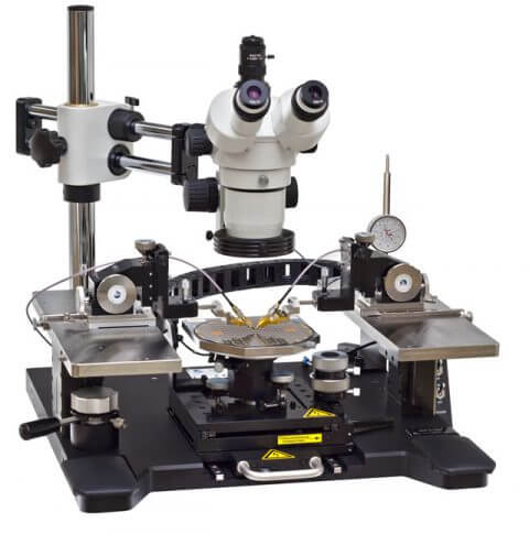
The EPS150RF and EPS200RF probe systems are application-focused packages that offer complete solution for best-in-class RF measurement results. Based on leading technology in RF probing and probe system design, and over 30 years of experience and application expertise, these solutions are the key to achieving accurate measurement results in the shortest time—with maximum confidence.
In our previous blog, we touched on the first two ways that these probe stations deliver accurate measurements results. To recap, they were:
1. Contact performance
2. Consistent calibration and measurement boundary conditions
In this post, we’ll cover the remaining three.
3. Accurate probe placement on calibration standards.
Accurate S-parameter measurements can only be obtained after determining the vector network analyzer (VNA) error coefficients. This step is also called “VNA calibration.” Various calibration methods are known and used in engineering practice depending on application requirements. In the commonly available SOLT method all standards must be fully known and specified.
In contrast to the coaxial or waveguide applications, actual frequency response of a planar standard critically depends on the probe placement. Implementation of special alignment marks can improve consistency of probe placement, but their use remains subject to operator interpretation. Subtle differences in probe placement seem inevitable, and limit calibration accuracy and reproducibility.
As a result, calibration residual errors caused by disagreement between the actual standard response and its definition may lead to misinterpretation of the DUT performance: inaccurate model parameters, over/under estimation of the figure of merits.
Dedicated probe-tip calibration available from WinCal XE™, such as LRRM method with automated compensation of the Load inductance variation, significantly minimizes impact of the probe misplacement on calibration and measurement results.
4. Verified calibration standards.
Establishment of a solid traceability chain for wafer-level RF measurement results is still underway. However, substantial achievements have already been made toward developing reliable methods for verification and comparison of planar calibration standards and wafer-level calibration methods.
Furthermore, implementing the calibration comparison technique developed in conjunction with NIST, the WinCal XE verification tool provides metrological-level analysis of calibration and measurement accuracy.
5. Dedicated wafer-level calibration methods.
Vector network analyzers do not provide the front-panel calibration methods optimized to wafer-level measurement needs, e.g. insensitivity to the probe placement and dispersion of characteristic impedance of CPW lines. Such methods are only available from the wafer-level calibration software WinCal XE.
For more information on the EPS150RF and EPS200RF probe stations, visit our website or download the technical review.