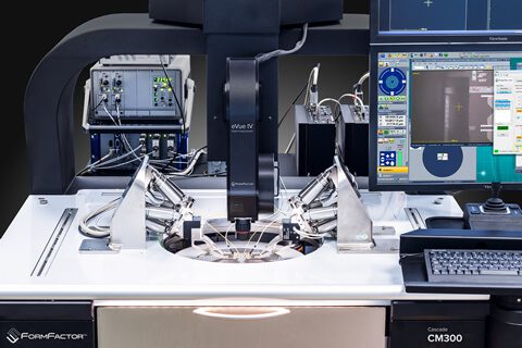
We recently announced new edge coupling features that enhance our silicon photonics (SiPh) solution for the CM300xi probe station. These features allow us to extend our ability to couple fibers to the edge of SiPh devices for both singulated die and on wafers, giving test engineers the capability to measure device performance consistent with native operating conditions. New machine vision techniques and in-situ calibration, along with integration of Keysight’s Test Automation Platform (TAP) software, and customers are able to more quickly accelerate products to market.
According to research from Inkwood Research, “the global silicon photonics market is projected to rise at a CAGR of 19.70% throughout the forecasting years of 2019-2027.” Enabling the rapid transfer of enormous amounts of data using optical signals instead of electrical signals, silicon photonics is continuing to gain momentum primarily with regards to data center and automotive applications.
The new edge capabilities provide engineers the flexibility to perform measurements optimized for their device designs and it expands our long-standing MeasureOne partnership with Keysight for silicon photonics applications. The new features include:
- Die and wafer-level edge coupling for photonic devices provides measurement capability that closely simulates device operation
- Advanced, in-situ optical positioner calibration with our OptoVue™ and OptoVue™ Pro for faster time to accurate measurement results
- Thermal range capability from -40 to 125°C in an enclosed environment
- In-situ power measurements of single fibers and fiber arrays to examine insertion path loss
- Integration of our probe station control and wafer-level measurement in Keysight’s N7700210C Wafer Prober TAP Plug-In software provides test steps that can be added to work-flow sequences without instrument-level programming commands
- Scalable platform with Keysight’s 77-Series photonic instruments, N437xE Lightwave Component Analyzers up to 110GHz, and PXIe based highly integrated modular DC and RF products shorten the test time of opto-electrical characterization
For more information on these new edge coupling features, check out the press release announcement.