Vertical Cavity Surface Emitting Lasers, better known as VCSELs, are an emerging technology with new applications in infrared lighting, proximity sensors, high-resolution video displays, atomic clocks and facial recognition technology.
VCSELs are semiconductor lasers in which the emitted light emerges perpendicular to the chip surface. A VCSEL is formed from a complex multilayer structure that is applied to the substrate by molecular beam epitaxy (MBE) or metal organic chemical vapor deposition (MOCVD). The epitaxial layers contain an active layer that generates the photons trapped between two Bragg reflectors (DBRs). The Bragg reflectors act as mirrors and the light is reflected back and forth several times through the active surface to improve amplification. In general, VCSELs generate an output power in the range of 0.5-5 mW and the most common emission wavelengths are in the range of 750-980 nm, as achieved with a GaAs/AlGaAs material system.
VCSEL arrays can be used to generate significantly higher powers. A 2D VCSEL array with thousands of emitters at a distance of a few tens of micrometers can emit several tens of watts of continuous radiation and thus compete with diode bars and even with diode stacks based on edge-emitting semiconductor lasers. The output power can be easily increased by increasing the number of emitters.
The advantages of VCSELs are low cost and optical efficiency with a relatively small footprint. They also have the advantage of wavelength stability over temperature. It’s also possible to combine a VCSEL wafer with a number of optical elements and then separate this bonded wafer instead of mounting the optical elements individually for each VCSEL. This creates the possibility of cost-effective, high-volume manufacturing of laser products. Another key advantage of VCSELs in comparison to edge-emitting semiconductor lasers is that they can be tested and characterized before the wafer is separated. This makes it possible to detect quality problems at an early stage.
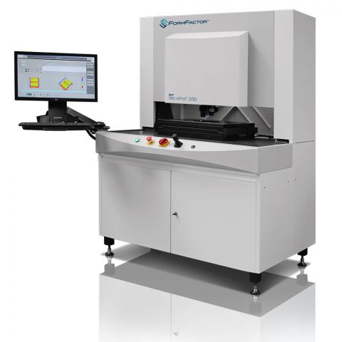
FormFactor has developed a high precision double-sided and thermally controlled probe system mainly for the VCSEL market.
Triple optics, including LIV (light intensity, current and voltage), near field and far field, can be mounted on top of the prober while probing is done from the bottom side of the wafer. The double-sided chuck design allows free access to both sides of the wafer. The wafer itself can be fixed by vacuum or mechanically clamped to allow testing up to the substrate edge.
The patented design of the thermally controlled probe unit (FireProbe) enables the test for both high and low temperature with very stable and accurate conditions. Both probe card and probe positioner types can be chosen for this new technology. Our extensive portfolio of high-performance probes suits most requirements.
There are choices of probe systems: a semi-automated double-sided probe system (PA200DSP) for R&D usage and a semi/fully automated double-sided probe system (PA200DS BlueRay) for production. PA200DSP has more flexibility of customization since there is greater access.
For more information on VCSELs, including technical componentry for wafer metrology, check out a past FormFactor blog – Vertical Cavity Surface Emitting Laser – VCSEL Technology Takes Off!