Vertical Cavity Surface Emitting Lasers, better known as VCSELs, are an emerging technology with new applications in infrared lighting, proximity sensors, high-resolution video displays, atomic clocks and facial recognition technology.
High-volume manufacturing of laser products possible
In general, the advantages of VCSELs are low cost and optical efficiency with small footprint. They also have the advantage of wavelength stability over temperature. In addition, it is possible to combine a VCSEL wafer with a number of optical elements and then separate this bonded wafer instead of mounting the optical elements individually for each VCSEL. This opens up the possibility of cost-effective mass production of laser products. Another key advantage of VCSELs in comparison to edge-emitting semiconductor lasers is that they can be tested and characterized before the wafer is separated. This makes it possible to detect quality problems at an early stage.
VCSEL – What is it actually?
VCSELs are semiconductor lasers in which the emitted light emerges perpendicular to the chip surface. A VCSEL is formed from a complex multilayer structure that is applied to the substrate by molecular beam epitaxy (MBE) or metal organic chemical vapor deposition (MOCVD). The epitaxial layers contain an active layer that generates the photons trapped between two Bragg reflectors (DBRs). The Bragg reflectors act as mirrors and the light is reflected back and forth several times through the active surface to improve amplification. In general, VCSELs generate an output power in the range of 0.5-5 mW and the most common emission wavelengths are in the range of 750-980 nm, as achieved with a GaAs/AlGaAs material system.
VCSEL arrays can be used to generate significantly higher powers. A 2D VCSEL array with thousands of emitters at a distance of a few tens of micrometers can emit several tens of watts of continuous radiation and thus compete with diode bars and even with diode stacks based on edge-emitting semiconductor lasers. The output power can be easily increased by increasing the number of emitters.
Modern surface measurement technology
For these different, challenging applications all-in-one solutions are most suitable. They need to be able to meet measurement requirements for a wide variety of processes and handle standard, thinned and bonded wafers as well as film frames. In addition, MicroProf® FS offers comprehensive measurement solutions for monitoring various compound semiconductor substrates such as GaAs, InP, SiC, GaN, ZnO and also transparent materials.
The technical solution
The MicroProf® FS is a fully automatic wafer metrology tool for a wide range of applications in various process steps, such as…
- for measurement of wafer thickness,
- bow and stress in epi process control
- as well as defect and haze mapping after epitaxy with high sensitivity to critical sub-micrometer defects,
- determination of critical dimensions (CD) and etching depth,
- thickness of dielectric layers, step height and width of metallization,
- taper of bond wafers and defect inspection of adhesive layers,
- TTV, thickness, roughness and Roll-of-Amount (RoA) after wafer grinding and
- acquisition of reflection spectra of Bragg reflectors (DBRs).
Due to its modular multi-sensor concept, the MicroProf® FS offers high flexibility and universality. This makes it ideally suited for a wide range of measurement tasks in VCSEL manufacturing. This is the essential point for VCSEL manufacturers who regularly adapt their research projects to new materials and the latest nano scientific concepts.
On the other side, the FormFactor FRT MicroProf DI optical inspection tool, enables inspection of structured and unstructured wafers during the entire manufacturing process. By combining 2D inspection and metrology, the MicroProf DI provides measurement solutions for a variety of applications, including defect inspection and wafer-level metrology for micro-bumps, RDL, overlay and through silicon via (TSV) in a single measuring tool.
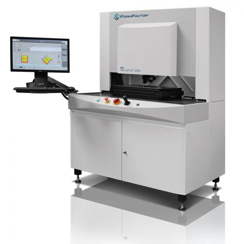
 The base component
The basic component is the established MicroProf 300®. This multi-sensor measuring tool enables both the measurement of wafers in different process steps and – through a hybrid measuring concept – to increase the accuracy of measurements on samples for which a single sensor or a single measuring principle is simply not sufficient. Depending on the task, these can be measurements with different topography and (layer) thickness sensors, which are fully automated by a single recipe. Controlled by the in-house software developed by FormFactor FRT, these sensors automatically combine different information and thus generate new information that is not directly accessible.
The software
The tool is operated by the SEMI-compliant FormFactor FRT Acquire Automation XT software. This software enables recipe-based measurements and complete data analysis, including automated determination of VCSEL parameters. Choose the appropriate measurement and evaluation routine for your measurement task from a variety of packages. For recurring structures, a layout wizard with a graphical user interface (GUI) can help you teach in the measurement positions. In addition, a fine alignment of the samples via pattern recognition is optionally possible.
This software offers comprehensive functions, from manual measurement on the tool to fully automatic measurement with one-button operation and integration into production control systems, e.g. via a SECS/GEM interface. You can easily configure different measurement tasks with different sensors to be executed consecutively as a measurement sequence. This also includes the execution of measurement, processing and analysis with intelligent algorithms, output and visualization of the results in the form of reports and the export of the results in different data formats. In addition, customers benefit from sample statistics and pass/fail classification at the wafer and die level.
The perfect workhorse
With a wafer handling system within an Equipment Front End Module (EFEM) and almost maintenance-free hardware components, the MicroProf® FS offers high throughput and is the perfect workhorse. The MicroProf® FS enables you to keep pace with the rapid progress of the VCSEL industry and quickly amortize your investment costs.