Today, industry icons and startups alike are investing heavily in a new use for superconductor technology. Namely, tackling the enormous challenges which threaten the future of the computing infrastructure needed to support our growing demand for data, computational power, and interconnected devices. Quantum computing, (based on qubits) promises to empower a whole new era of artificial intelligence, complex system optimization, molecular modeling for medicine, cryptography, and much more. Cold superconducting CPUs using RSFQ (rapid single flux quantum), RQL (reciprocal quantum logic), or similar new logic families promise to slash the huge energy and heat issues limiting the growth and location of HPC (high performance computing) supercomputers and hyperscale data centers.
These new cryogenic processors need memory, and to maintain their energy benefits the memory systems must also be cold. Superconducting memory may be years away, however, studies show that traditional CMOS DRAM structures can be very effectively used at cryogenic temperatures such as 77K. Cryogenic wafer testing is required to tune the process and qualify memory components for use at these temperatures.
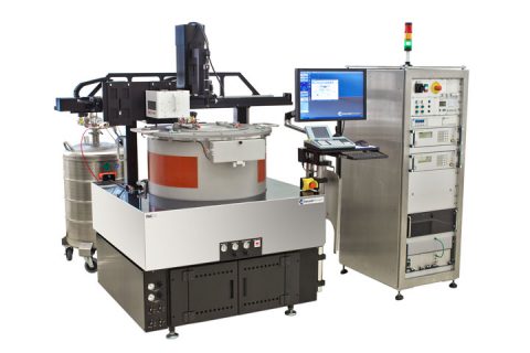
The PAC200 semi-automated cryogenic probe station is the ideal solution for automatic testing of wafers and substrates up to 300 mm in a cryogenic environment down to 77 K with liquid nitrogen or below 20 K with liquid helium. It supports a wide range of applications, including DC and RF measurements of the latest silicon, compound semiconductor and superconductor devices. The probe platen is designed to mount probe cards or up to eight vacuum-type positioners on magnetic feet. To reduce heat entrance, probes or probe cards are thermally anchored to the cryogenic shield. A high-resolution video microscope with 50 mm x 50 mm travel range is mounted either on a microscope mount with swivel or on a microscope bridge for vibration-sensitive test applications and additional test instruments.
Here are some noteworthy features and benefits that make the PAC200 probe system flexible, stable, and easy to use:
- The system is customized to user’s requirements
- It provides different substrate carriers for wafers up to 300 mm or single dies
- The motorized stage provides programmable stepping for testing multiple dies across the wafer
- Velox™ probe station control software automates testing and boosts productivity
- The system delivers a wide range of electrical measurements (I-V, C-V, two-port, multi-port and differential RF)
- RF tests are supported by a wide range of probes and calibration tools, such as calibration substrates and WinCal XE™ calibration software
- Other test equipment can be implemented (e.g. infrared sources and optics)
- The vacuum chamber and heat shield provide ice- and condensation-free probing down to 77K (liquid nitrogen) or below 20 K (liquid helium)
- The platen supports up to 8 thermally anchored, movable probe positioners, or easily exchanged probe cards for high probe count
- Highly stable mechanics with vibration isolation table delivery high probe placement accuracy – ideal for small pads
- It has a simple, straightforward design for easy and ergonomic operation
For more information, be sure to visit the cryogenic probing section of our site or download the PAC200 data sheet.