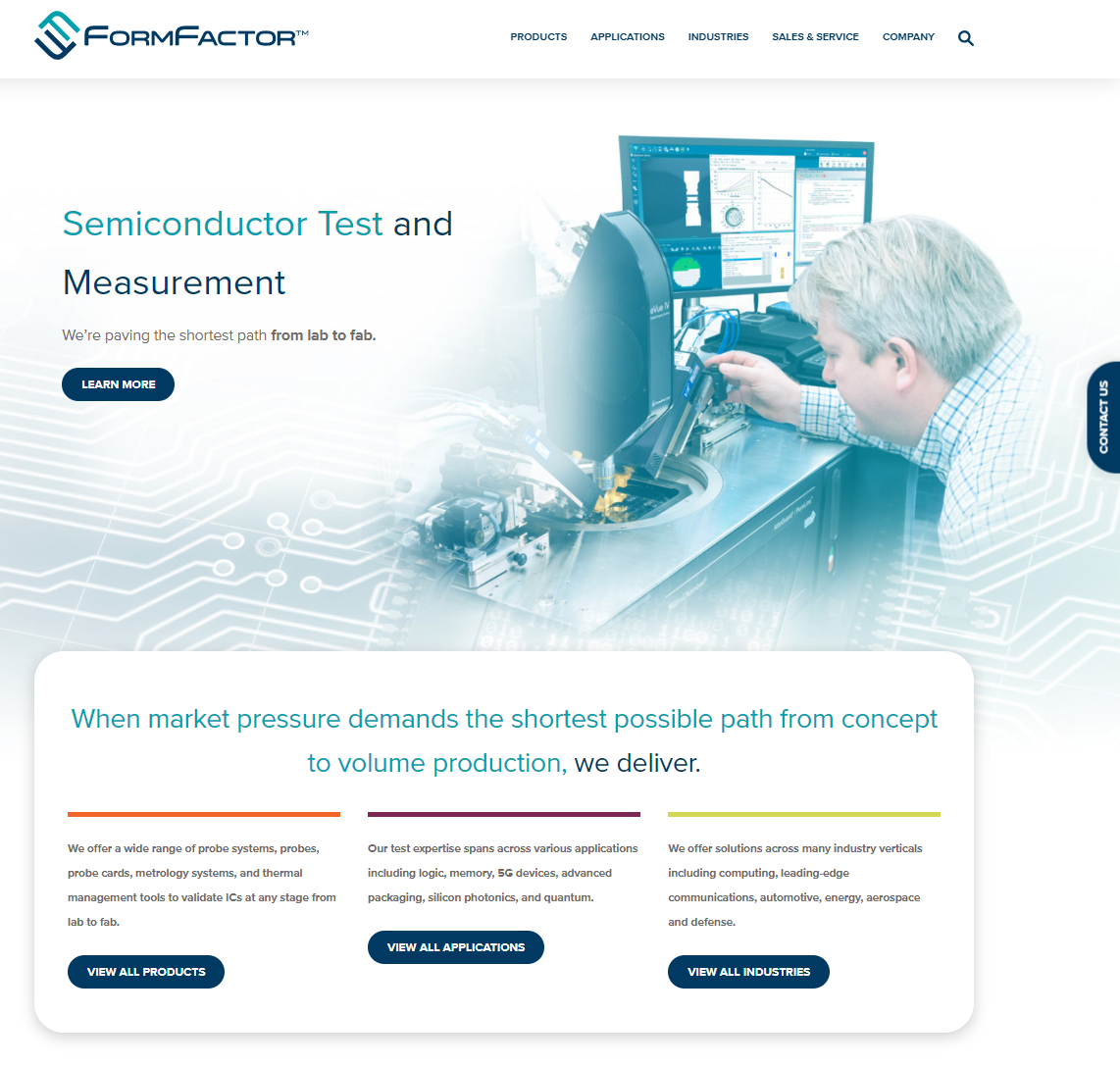
We recently launched an updated version of our website, and this version brings you some enhanced search functionality to allow you find the right solution for your needs. In addition to enhanced search functionality, we have also introduced two entirely new sections – Applications and Industries.
New Section: Applications
The applications section of our new site breaks down our products into the wide range of test and measurement applications in which they are applicable. There are many:
Semiconductor Research and Development
- DC Parametric Test – Accurate and repeatable DC parametric measurements (IV, CV, pulsed, and high-power) reduce uncertainty. Trustworthy results accelerate device qualification and produce more precise models and design toolkits. In turn, these allow designers to deliver more competitive products to market faster.
- Low Frequency Noise – Accurately measuring low frequency noise (LFN) at wafer level has become even more critical for advanced high-speed, low power technologies found in newer 5G devices and nanoscale transistors.
- Power Semiconductors – Next generation power devices are rapidly being developed to bring down end-user device costs and support a wide range of growing application performance needs.
- RF/mmW and 5G – Engineers developing 5G are looking at phased arrays and may have >60 radio frequencies to handle in the same device, which places an enormous technical and economic load on manufacturers’ automated test equipment and processes.
- Terahertz – Research into new materials and semiconductor technology is pushing existing test frequency boundaries to terahertz (THz) extremes.
- mm-Wave Load-Pull – FormFactor has partnered up with Focus Microwaves and Keysight Technologies to deliver a fully integrated solution for accurate on-wafer mm-Wave load-pull measurements.
- Silicon Photonics – The semiconductor industry is at the gateway of a technology shift in the form of silicon photonics (SiPh), which holds the potential for spectacular gains in speed, power efficiency and density.
- VSCELs and MicroLEDs – Optical technologies, such as VCSELs and MicroLEDs, create new possibilities that are securer, safer, and smarter.
- Quantum Computing – Quantum computers stand poised to deliver dramatic breakthroughs in many scientific and engineering fields.
- Cryogenic Devices – The use of on-wafer superconducting materials, other novel materials and traditional semiconductors at cryogenic temperatures (below about 123K, or -150°C) has risen markedly in recent years.
High Volume Manufacturing
- Foundry and Logic – AI, HPC, and the proliferation of consumer electronics are driving the development of next generation advanced logic technologies.
- DRAM and Flash Memory – Increased data consumption and the growing proliferation of memory device applications are driving the demand for DRAM and Flash memory.
- Advanced Packaging – As companies explore advanced packaging techniques, their search leads them to seek out cost effective testing solutions to move to high volume production.
- RF/mmW and 5G – The promise of 5G is significantly greater mobile speeds for real-time connectivity for mission-critical applications.
- AI Processors – Artificial Intelligence (AI), once the stuff of science fiction movies, now comes in many guises, from personal assistants in cell phones to individualized movie recommendations to drone-based pipeline inspections.
- Optical Test – FormFactor’s family of optical device probe cards offer customized solutions for testing CMOS image sensors and LED devices.
- Parametric Test – Parametric testing, or wafer acceptance test (WAT), is a unique application for IC manufacturers to ensure that the wafer production process is consistent and maximizes yields.
- Cryogenic Devices – The use of on-wafer superconducting materials, other novel materials and traditional semiconductors at cryogenic temperatures (below about 123K, or -150°C) has risen markedly in recent years.
Metrology Applications
- Advanced Packaging – With new chip packaging techniques, including 2.5D, 3D-IC, fan-out wafer-level packaging and system-in-package, the need for flexibility in wafer metrology and handling has exploded.
- Semiconductor and MEMS – FormFactor’s high-quality, fully automated, multi-sensor FRT metrology technology helps wafer manufacturers control process tolerances and maintain their required quality standards.
- Medical Technologies – Optimizing product quality in medical technologies is a critical requirement for medical device manufacturers.
- Automotive and Industrial – FormFactor’s FRT measuring systems provide fully automated data about topography, step height, roughness, flatness, layer thickness and many other parameters – contact-free and non-destructive.
Partner Solutions
To deliver high-performance, high-throughput test results for challenging applications in the engineering lab, FormFactor collaborates closely with MeasureOne partners. Together, we develop, configure, and install industry-leading solutions with proven performance and top-tier support. These on-wafer test and measurement solutions reduce risk, control costs, and bring products to market faster.
New Section: Industries
FormFactor products ensure the quality and reliability of ICs used in electronics affecting every aspect of our lives. Here are some of the industries we support:
We hope you find our new website easy to use and navigate as well as informative!