The use of on-wafer superconducting materials, other novel materials and traditional semiconductors at cryogenic temperatures (below about 123K, or -150°C) has grown quickly in recent years. Inventive new sensors take advantage of unique material properties at very low temperatures to detect a wide variety of physical phenomena such as infrared radiation, magnetic fields, x-rays, and more. These have applications in a number of industries such as health care, defense, industrial automation, and astronomy. Recently, developments in the field of quantum computing and superconducting logic are delivering bold energy and performance gains for the future of computing. And there will undoubtedly be many more cryogenic applications and devices.
High-performance thermal imaging, for one, is widely used today in surveillance/security, night vision, remote sensing, meteorology, military threat and target detection, body heat analysis, astronomy, and more. These systems use FPAs (focal plane arrays) based on cooled IR sensors. Cryogenic environments help reduce thermal noise so that these detector arrays can deliver improved resolution and sensitivity.
Cooled IR sensors are built from different materials to target various wavelength ranges from the near infrared (NIR) through long wave infrared (LWIR), including silicon, numerous III-V compounds (InGaAs, InSb, InAsSb, InAs/GaSb, etc.), often designed as quantum well photo detectors, MCT (mercury cadmium telluride), and superconducting photon detector technologies including YBCuO, GdBO3, MgB2, and more. Testing these low-temperature technologies on-wafer requires a cryogenic probe system.
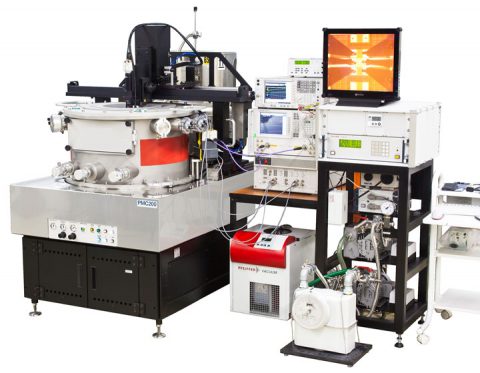
The cryogenic test apparatus is enclosed in a vacuum chamber to provide a suitably sealed and evacuated environment. Temperatures of 77 K or even lower are reached by a constant liquid nitrogen or liquid helium flow or with an alternative cooling technology. Additionally, the cryostat itself contains resistive heaters, cryogenic grade temperature sensors and a temperature controller to provide superior stability of this thermal system over a wide temperature span. Signal feedthroughs, optics for cameras, and probe positioner controls all require special considerations for access to the extreme vacuum/cold environment. Safety, vibration, and sample mounting also present new challenges for vacuum/cryogenic conditions. Even the probes must be designed for use at cryogenic conditions. Finally, although many solutions are available for single small diced samples with just a few signals, process and product qualification requires a higher class of tools. High volume testing demands a large chamber for full wafer samples, multi-channel cryogenic probe cards, a software-controlled wafer stage for step-and-repeat testing across the wafer surface, and other capabilities to maximize test throughput.
We are ahead of the pack for high-throughput cryogenic wafer test, with this unmatched combination of powerful features:
- Step-and-repeat automation with programmable, motorized XYZΘ stage.
- Automatic camera-based alignment adjustments at each step.
- Up to 8 easily positioned and very stable cryogenic probes for DC, RF, and optical signals – and probe cards for even higher signal count.
- Sample sizes from fragments up to full 200mm wafers (300mm option available).
- Wafer exchange without disrupting probes or probe cards.
- Programmable, motorized positioning of multiple black-body radiation sources, microscopes, and other equipment
High test throughput enables our customers to move from lab concepts to device characterization to design debug to high-volume engineering/production test. Our lineup, the PAC200 probe station, PMC200 probe station, and PLC50 probe station, includes multiple size and automation levels, and flexible/customizable configurations.