Adhesives are key components in semiconductor-based devices. The glues are used to bond, contact, and encapsulate wafers, chips and other microelectromechanical components on printed circuit boards.
In the semiconductor industry, Glue Bonding or Adhesive bonding is a wafer bonding process in which substrates of different types of materials are connected with applying an intermediate layer – the glue layer.
The characterization of the bonded wafers is essential because it determines the process quality or the quality of the fabricated devices. Along with destructive techniques for the bond strength evaluation, like tensile or shear testing, optical measurements are often the choice of means. These non-destructive optical methods find defects like cracks or voids in different layers and characterize bond layer (adhesive) homogeneity.
The FormFactor FRT IRT sensors were developed for the thickness measurement of materials that are transparent in near infrared light. The IRT is an interferometric film thickness sensor with an infrared light source. Measurements can be conducted as single point and profile measurements, or film thickness mappings of larger areas. These sensors are mainly used to determine wafer thicknesses very precisely. But it is also possible to characterize single layers of multi-layer systems.
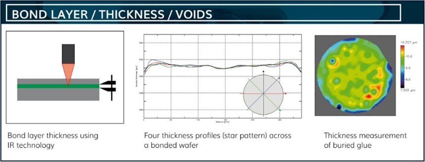
Measurement of Bond Layer Thickness
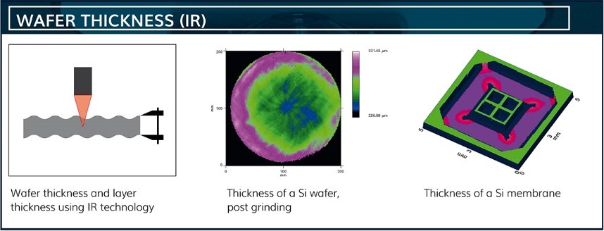
Measurement of Wafer thickness and Membrane thickness
The newest generation of FormFactor FRT IRT 800 sensor offers major advantages:
First, the size of sensor electronics is reduced, so there is more space available in the tool. Further, smaller structures, like scratches or voids, can be measured because the lateral resolution improved up to 5.5 μm.
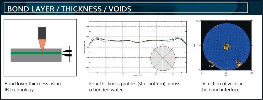
Detection of voids in bond layer
With the extended film thickness measuring range up to 3200 μm, it is possible to measure 55 μm thicker layers. The maximum silicon thickness which can now be measured is approximately 850 μm.
The calculation: the measuring range needs to be divided by the refractive index of material (n), e.g., standard silicon wafers have a refractive index of n ≈ 3.6 (3200 μm/ 3.6 ~880 μm).
For thin films (4-300um/n), FormFactor offers the FRT IRT 80 sensor.
The absolute highlight is the speed with which the IRT 800 sensor conducts the film thickness measurement: now five times faster with 20.000 measurements / sec. (20 hHz)!
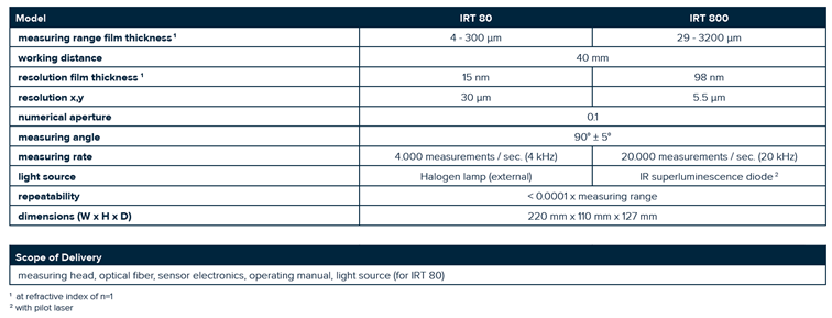
All parameters are shown in the table below.
Here’s a video demonstrating bonded wafer measurement: