The increasing desire for energy efficiency across various domains such as systems, cars, consumer appliances, portable electronics, and their integration with the Internet of Things, is propelling the rapid progress of power semiconductor devices. This is leading to an unprecedented surge in demand, setting new record highs year after year.
Consequently, companies and foundries worldwide are ramping up their test capacities in research and development, high-performance device production, and general high-volume manufacturing. The rapid development of next-generation power devices aims to reduce end-user device costs and cater to the growing demand for enhanced application performance.
According to industry reports, back in 2017, approximately 68% of power devices in power electronics were designated for low voltage applications (<900 V). However, the remaining segment (32%) has been experiencing significant growth and is divided by voltage into three categories: medium (1 – 1.9 kV), high (2 – 3.3 kV), and very high (>3.3 kV) voltage applications.
Two areas witnessing an expansion in the utilization of power semiconductor devices/modules are electric vehicles and transportation. These areas require higher current handling capacities (200 – 400 A), elevated voltages (3.3 – 10 kV), and operation at higher temperatures (300 – 400° C) to meet new reliability and performance standards. As a result, extensive research and development, device characterization, and manufacturing test development are necessary.
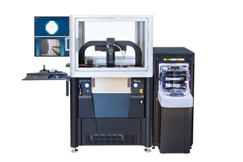
One key challenge for power IC engineers is testing on-wafer instead of in-package. FormFactor is playing a significant role in on-wafer power semiconductor test, addressing this challenge effectively with the TESLA200 and TESLA300 Advanced On-Wafer Power Semiconductor Probing Systems. These probe systems cater to power semiconductor researchers, device/test engineers, and manufacturing managers/operators.
With the TESLA systems, users can gather precise high voltage and high current measurement data while ensuring complete operator safety. Whether working with single or volume thinned wafers, the systems enable fast and efficient testing for purposes like research and development, device characterization/modeling, and niche production.
These cutting-edge systems facilitate easy setup and introduce new testing capabilities, accommodating both static and dynamic high-power measurements along with ultra-low leakage device testing. Moreover, they offer full temperature support ranging from -55° to 300° C and beyond.
Designed with multiple anti-arcing technologies, the TESLA200 and TESLA300 ensure high-voltage test performance without compromising device protection, boasting impressive capabilities of up to 10,000V DC. The integration of materials and technologies with low contact and thermal resistance further enhance the systems, allowing for exceptional high-current measurements of up to 600A.
To provide a comprehensive solution, FormFactor offers an extensive selection of high-voltage and high-current probes, along with anti-arcing probe cards. The system also supports high-power test equipment for engineering and production purposes. Furthermore, it comes in various versions, including manual, semi-automatic, and now fully-automatic, delivering accurate data in the shortest possible time.
For more information, visit our high-voltage, high-current applications page on our website.